Controller Independent Flash Recovery
It is almost 2011 and the data recovery world has changed drastically in the last several years with the increasing demand and decreasing price of solid state flash-memory based devices. Data recovery on flash media circa 2005-2006 consisted of the physical repair of damaged circuit boards on devices such as USB Thumb Drives, SD Cards, CompactFlash Cards, etc… Damaged circuits could be repaired, crystal oscillators could be swapped and the actual NAND Flash Memory could be removed and placed on an identical, working device.
Slowly, as more and more manufacturers got into the solid state game the more we found it nearly impossible to find exact matches on devices anymore due to the fact that most OEM’s grabbed PCB’s from the cheapest Taiwanese or Malaysian supplier. It got to the point where an individual could purchase 2 flash drives at the same time and while identical-looking from the outside, they would have completely mismatched internal components. This caused us to start researching ways to read the flash memory chips independent from the rest of the circuitry and controller.
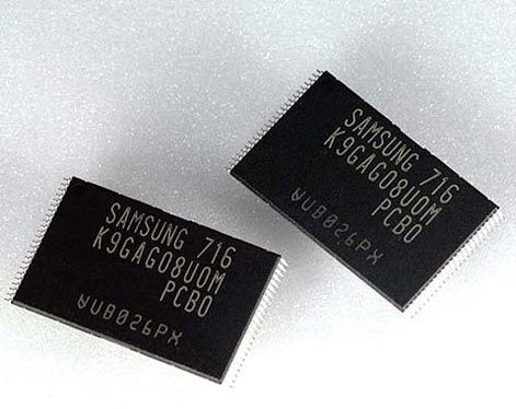
TSOP-48 Chips
We began to inquire about NAND programing devices and were eventually easily able to read the flash memory into an image file on our lab computers. However, most of the time, the data looked like a garbled mess and the blocks of data were in the incorrect order and dispersed throughout the image. The reason for this is that the flash memory controller chip on the PCB of the flash device controls various aspects of the NAND memory including wear-leveling algorithms, which ensure that each block on a flash memory chip will be used evenly as to not wear out and blocks prematurely. The controller then translates this information and makes the data readable at the user level. It is no wonder that the image files we were extracting did not look like a standard hard drive image. Just as hard drives have a ‘service area’ which handles the data on the platter surface and translates it into readable data, these flash devices have this information stored in each sector as well.
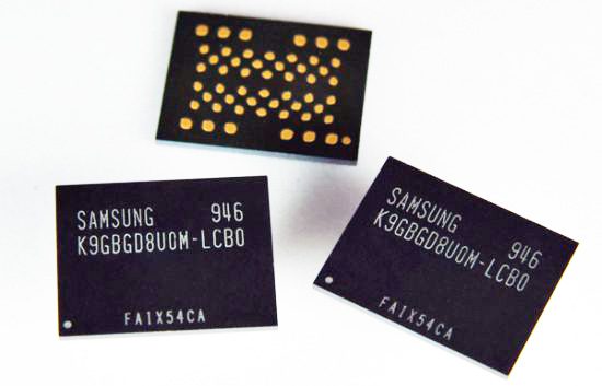
TLGA Chips
Starting by looking at patterns in the image files we were able to determine that there are markers in the ‘service area’ of each sector that tells us what order the blocks go in. Also, while looking at the FAT tables, we found out that the images are mixed up across chips kind of like mini high-end RAID systems. The number of chips increases the complexity of assembling the image dramatically. SSD Drives can have a dozen individual chips, so the process can be very time consuming and labor intensive.
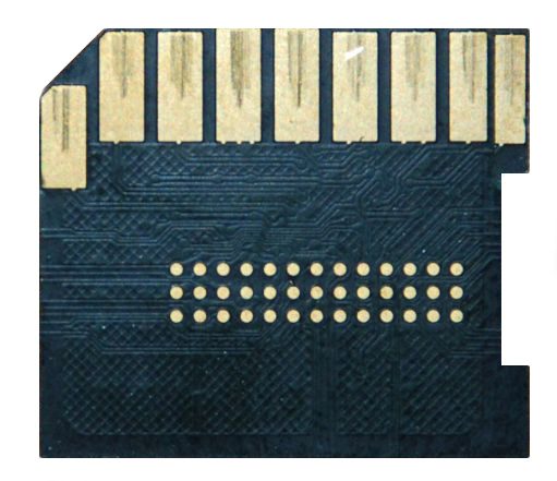
Monolithic Chip
To further complicate the issues, NAND manufacturers are trying to make their devices smaller and smaller in physical size while getting larger and larger in storage capacity. When we first started with our Flash Recovery R&D we only saw TSOP-48 NAND flash memory-based devices. Now we see various monolithic chips which contain both the controller and the NAND memory integrated on the same chip, as well as TLGA chips which are BGA Surface mount chips with a different pinless layout. We have developed circuit boards and methods for reading both new types of flash memory. Even more recently we are seeing Samsung’s MoviNAND chips used in Flip Camcorders and Amazon’s Kindle.
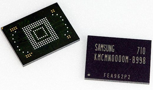
moviNAND eMMC chips
So, our research and development is ever-evolving in the realm of Flash recovery. I hope this illustrated the complexity of flash-based recovery and how it is still an emerging and evolving technology. Almost 7 years ago when Flashback Data was started, we saw this evolution from hard drive to flash-based media. Why do you think we called ourselves Flashback Data?